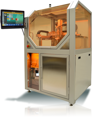
A full solution for coating semiconductor wafers with uniform thin films of photoresist in applications where traditional high speed spin coating cannot provide uniform coverage of deep well topographies or high aspect ratios such as MEMS. Designed for 100, 150, 200, and 300mm (option) semiconductor wafer processing.
Visit How Ultrasonic Nozzles Work to learn more about the unique capabilities of ultrasonic spray.
SPT200 openSPT200 side viewSPT200 close upSPT200 WS single wafer handlerSPT WS wafer handler interiorSPT200 Ultrasonic Photoresist Coating System
Glass & Industrial
Basic Specifications
| Dimensions: 1066mm W x 1765 mm H x 1095 mm D (42” W x 70” H x 43” D) |
| Work Area: 465 mm x 465 mm x 100 mm (19.7” x 19.7” x 3.9”) |
| Control: Windows-based (pc included 19-inch touch screen interface) |
| Power Requirements: 208-240VACc, 16A max, 50/60 Hz 1 phase (L,N,G) or (L1, L2, G) |
| Air: 551.6 kPa (80PSI) 1 compressed air, 1 nitrogen |
| Motors: Brushless DC Servo |
| Certification: CE |
| Ultrasonic Nozzle Designs: Vortex, AccuMist, Impact |
System Options
| Heat and/or Vacuum Plate: Standard Option |
| Head configuration: Up to two heads |
| Liquid Delivery: Common Liquid Delivery: Syringe pump (standard, Sonic or stirring), MicroFlow, SonoFlow Fusion |
